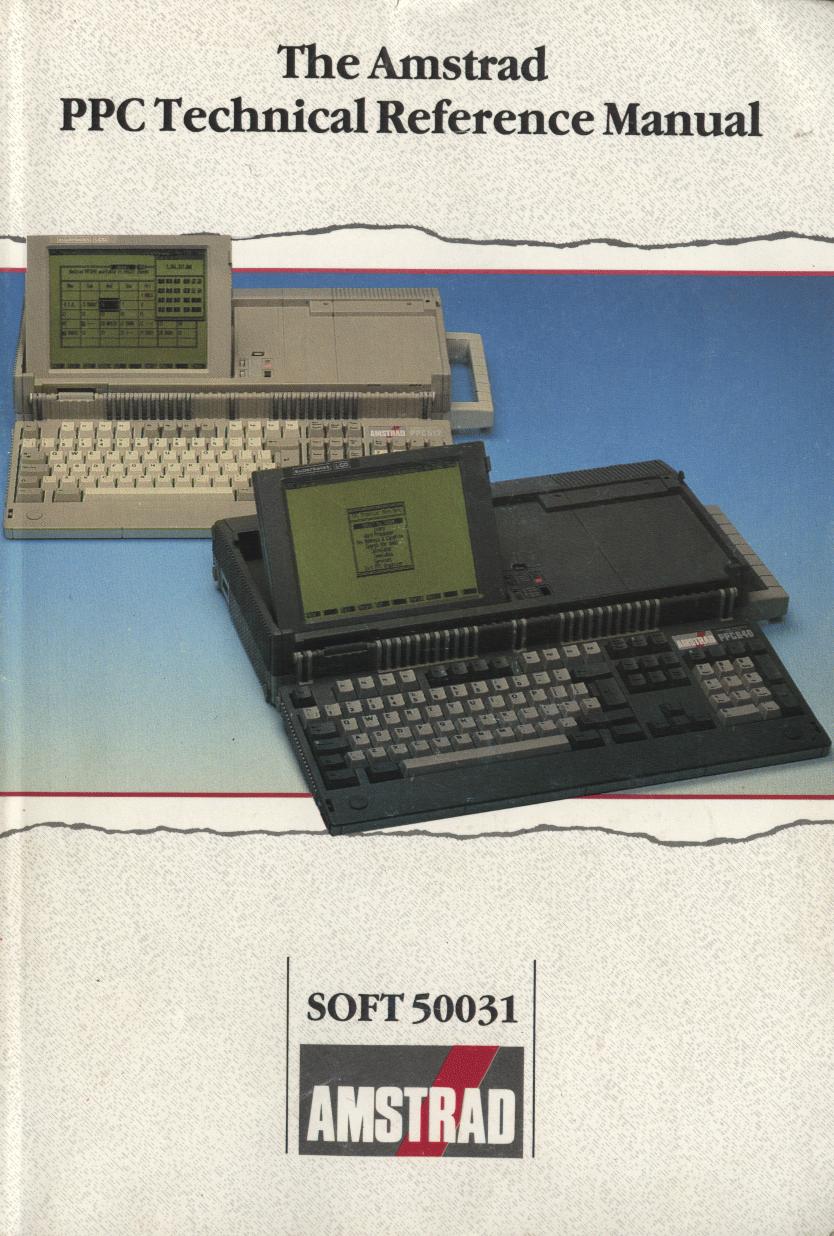
Preface
This Technical Reference Manual is intended primarily to assist writers of software for the Amstrad PPC, although in conjunction with the PPC Service Manual it will be of interest to designers of add-on hardware.
It is assumed that the reader has a working knowledge of the Industry Standard architecture comprising of an 8086 (or 8088) with DMA, PIT, RTC and Interrupt Controller support chips; plus Colour Graphics Adapter (or Monochrome Graphics Adapter) with Floppy Disk, Serial and Parallel Adapters.
The information contained herein is largely unique to this document, with the exception of parts of the appendices which expand on the information contained in the PPC User Instructions and the Microsoft MSDOS Reference Manual.
Whilst the PPC implements a superset of the Industry Standard, this manual makes no attempt to identify those areas of the PPC specification which exceed the Industry Standard. Users should, therefore, exercise caution when writing software for a range of manufacturers' PCs and only use the "Lowest Common Denominator" facilities if simple portability is required.
Please note, that communications regulations do not allow the release of technical information relating to the circuitry or construction of the PC2000 modem.
© Copyright 1988 Amstrad Consumer Electronics Plc
Neither the whole nor any part of the information contained herein, nor the product described in this manual may be adapted or reproduced in any form except with the prior approval of Amstrad Consumer Electronics Plc ('Amstrad').
All information of a technical nature and particulars of the product are given by Amstrad in good faith. However, it is acknowledged that there may be errors or omissions in this manual.
All correspondence should be addressed to:
Amstrad Consumer Electronics Plc
Brentwood House
169 Kings Road
Brentwood
ESSEX CM14 4EF
All maintenance and service on the product must be carried out by Amstrad authorised dealers. Amstrad cannot accept any liability whatsoever for any loss or damage caused by service or maintenance by unauthorised personnel. This manual is intended to assist the reader in the use of the product, and therefore Amstrad shall not be liable for any damage or loss whatsoever arising from the use of any information or particulars in, or any error or omission in, this manual or any incorrect use of the product.
Written by Bill Weidenauer and edited by Susan Vass, Amstrad plc.
Published by Amstrad.
First Published 1987.
MS-DOS(R) is a registered trademark of Microsoft(R) Corporation
Amstrad is a registered trademark of Amstrad plc.
Unauthorised use of the trademark or the word Amstrad is strictly forbidden.
Table of Contents:
Section 1 - Hardware
Amstrad PPC Technical Manual
This manual provides a comprehensive description of the Amstrad PPC hardware and firmware. General information about the PPC and the delivered operating system software is contained in the Amstrad PPC User Instructions. This manual is intended to satisfy the needs of advanced developers who must have access to the various resources available within the PPC640 and PPC512.
Note that all address constants in this document are hexadecimal. In addition hexadecimal quantities are noted with small letter 'h' terminator to denote that they are in hexadecimal form. Address quantities are not usually annotated this way since they are clearly hexadecimal. Values are presented in hexadecimal form when they are logically bit oriented quantities rather than of purely numerical significance.
The CPU is a low power 8086-2 microprocessor with 1 Megabyte memory addressing capability (See Figure 1.1), running at a clock frequency of 8MHz. The CPU is connected to an on-board 16-bit system memory bus requiring four 125nS timing cycles (T-States) per access resulting in a 500nS memory cycle for 16-bit memory. The CPU is also connected on an on-board 8 bit I/O and memory peripheral bus with a 4 MHz clock, which in turn connects to an external expansion bus. Operations on the 8-bit bus automatically incur 125nS wait states as follows:
| Operation |
Wait States |
Bus Cycle |
| 8-bit (Memory) |
4 |
1.0 μS |
| 16 to 8-bit convert (Memory) |
12 |
2.0 μS |
| 8-bit (I/O) |
6 |
1.25 μS |
| 16 to 8-bit convert (I/O) |
16 |
2.5 μS |
The CPU is configured to run in maximum mode and the instruction set may be optionally extended by the addition of an 8087-2 Numeric Data Coprocessor. The 8087 BUSY output is connected directly to the 8086 NOT TEST input.
The main board memory consists of 640K bytes of system RAM with parity checking and 16K bytes of system ROM without parity checking.
The 640K byte user RAM starts at CPU memory address 00000 and extends to 9FFFF. Note that the PPC512 has 512K bytes installed memory ending at address 7FFFFh and the address space from 80000h to 9FFFFh may be extended in external 32K byte blocks (up to the 640K maximum).
The 128K byte address space from A0000 to BFFFF is reserved for video regeneration buffers, and is not used by CPU programs. The PPC Internal Display Adapter (IDA) uses the 64K byte address range from B0000 to BFFFF. The segmentation of this memory range is dependent on the display mode (See section 1.11). External display adapters also use this memory address range for their display buffers.
The 192K byte address space from C0000 to EFFFF is reserved for external expansion ROM address space. Hard Disk controllers use the range from C8000 to C9FFF. Additional hard disk controllers may also use the area from CA000 to CD000. The PPC test board uses the ROM area from E0000 to E7FFF.
The 16K byte system ROM is at FC000 to FFFFF and contains the Resident Operating System (ROS) firmware. The 48K byte address range from F0000 to FBFFF is reserved for ROM space expansion. The 16K byte ROS area address bits are partially decoded such that the ROS ROM repeats four times in the F0000 to FFFFF address range.
MEMORY LAYOUT
| 00000 |
|
ON-BOARD
DYNAMIC RAM
|
640K Byte
System Memory
|
| |
|
9FFFF |
| A0000 |
128K BYTES
VIDEO DISPLAY BUFFERS
|
|
| BFFFF |
1M BYTE
ADDR
RANGE |
C0000 |
192K BYTES EXPANSION ROMS
|
| EFFFF |
| |
|
F0000 |
48K BYTES ROS ROM BLOCK REPEATS
|
64K Byte
System ROM
area
|
| FBFFF |
| FC000 |
16K BYTES (ROS)
RESIDENT OPERATING SYSTEM ROM
|
|
|
| FFFFF |
|
The interfaces on the main board occupy the 8086 I/O addresses as follows:
| ADDRESS(hex) |
OUTPUT USE |
INPUT USE |
| 000 - 00F |
8237 DMA Controller |
8237 DMA Controller |
| 010 - 01F |
Do Not Use |
Do Not Use |
| 020 - 021 |
8259 Interrupt control |
8259 Interrupt control |
| 022 - 03F |
Do Not Use |
Do Not Use |
| 040 - 042 |
8253 PIT Load Count (0-2) |
8253 PIT Read Count (0-2) |
| 043 |
8253 PIT Load Mode |
Undefined |
| 044 - 05F |
Do Not Use |
Do Not Use |
| 060 |
No Effect |
Port A - Keyboard Code or System Status 1 |
| 061 |
Port B - System Control |
Port B - (Readback) |
| 062 |
No Effect |
Port C - System Status-2 |
| 063 |
No Effect |
Do Not Use |
| 064 |
Write System Status-1 |
Do Not Use |
| 065 |
Write System Status-2 |
Do Not Use |
| 066 |
System Reset |
Do Not Use |
| 067 - 06F |
Do Not Use |
Do Not Use |
| 070 |
146818 RTC Address |
Do Not Use |
| 071 |
146818 RTC Data |
146818 RTC Data |
| 072 - 077 |
Do Not Use |
Do Not Use |
| 078 |
Reserved |
Reserved |
| 079 |
Do Not Use |
Do Not Use |
| 07A |
Reserved |
Reserved |
| 07B - 07F |
Do Not Use |
Do Not Use |
| 080 |
Do Not Use |
Do Not Use |
| 081 |
DMA Page Register Ch 2 |
Do Not Use |
| 082 |
DMA Page Register Ch 3 |
Do Not Use |
| 083 |
DMA Page Register Ch 0,1 |
Do Not Use |
| 084 - 09F |
Do Not Use |
Do Not Use |
| 0A0 |
NMI Mask Control |
Do Not Use |
| 0A1 - 0BF |
Do Not Use |
Do Not Use |
| 0C0 - 0FF |
Reserved |
Reserved |
| 2F8 - 2FF |
Modem UART Tx
Data/Control |
Modem UART Rx
Data/Control |
| 378 |
Printer Data Latch |
Printer Data Latch |
| 379 |
Do Not Use |
Printer Status |
| 37A |
Printer Control Latch |
Printer Control Latch |
| 37B - 37F |
Do Not Use |
Do Not Use |
| 3B0 - 3B7 |
Mono Mode CRTC
Registers |
Mono Mode CRTC
Registers |
| 3B8 - 3BF |
Mono Mode Control
Registers |
Mono Mode CRTC
Registers |
| 3D0 - 3D7 |
Colour Mode CRTC
Registers |
Colour Mode CRTC
Registers |
| 3D8 - 3DF |
Colour Mode Control
Registers |
Colour Mode Control
Registers |
| 3F0 - 3F1 |
Do Not Use |
Do Not Use |
| 3F2 |
Drive Selection |
Do Not Use |
| 3F3 |
Do Not Use |
Do Not Use |
| 3F4 |
Do Not Use |
765 FDC Status |
| 3F5 |
765 FDC Data |
765 FDC Data |
| 3F6 - 3F7 |
Do Not Use |
Do Not Use |
| 3F8 - 3FF |
COM1 8250 UART Tx
Data/Control |
COM1 8250 UART Rx
Data/Control |
The 8086 CPU I/O addresses on the expansion bus are as follows:
| ADDRESS(hex) |
USE |
| 200 - 20F |
External Game Control Interface |
| 210 - 217 |
External Bus Expansion Unit |
| 220 - 24F |
Reserved |
| 278 - 27F |
External Printer Port |
| 2F0 - 2FF |
Reserved |
| 300 - 31F |
External Prototyping Card |
| 320 - 32F |
External Hard Disk Controller |
| 380 - 38F |
External SDLC Serial RS232C Port |
| 3A0 - 3AF |
Reserved |
| 3B0 - 3BB |
External Monochrome VDU Controller |
| 3BC - 3BF |
Printer Port |
| 3C0 - 3CF |
External Graphics Controller |
| 3D0 - 3DF |
External Colour/Graphics Controller |
I/O address above 03FFh, if accessed, wrap around and are mapped onto the range 0000h-03FFh.
External cluster controllers at 0790h-0793h, 0B90h-0B93h, 1390h-1393h and 2390h-2393h wrap around to I/O addresses 0390h-0393h respectively.
The Amstrad PPC supports four DMA channels on the system board, using an 8237-4 DMA controller and programmable page registers to extend its addressing range from 64k bytes to the full 1M byte processor address range. Each channel is able to transfer data in blocks of up to a maximum of 64K bytes within a page. The DMA channels are for 8-bit data transfers between (8-bit) I/O devices and 8-bit or 16-bit memory.
In peripheral (slave) mode, CPU I/O address lines A0 - A3 are connected conventionally so that 16 command codes appear in the order described in the 8237 data sheets (See section 3.5).
The DMA controller CLK is driven at 4MHz (+/- 0.1%). In master mode during DMA transfers on channels 1,2 and 3, one wait state is added resulting in a five-clock DMA bus cycle of 1.25μS. Channel 0 transfers have a four-clock bus cycle of 1μS.
The DMA channel request signals are as follows:
| DMA Channel |
USE |
| 0 |
8253 Timer/Counter OUT1 output - for memory refresh. |
| 1 |
Spare for use by expansion bus. Used by external SDLC Serial Port. |
| 2 |
765 Floppy Disk Controller DRQ output. Available on the expansion bus. |
| 3 |
Spare for use by expansion bus. Used by external Hard Disk Controller. |
DMA channels 1, 2 and 3 can address the entire 1M byte addressing range of the CPU through the use of their associated DMA page registers. There are three DMA registers, one each for channels 1 through 3. Each page register defines for its channel which one of sixteen 64K byte pages in the 1M byte address range DMA transfers are to occur. The page registers are static so that modulo 64K byte addressing occurs at page boundaries.
The DMA page register bit assignments are as follows:
| Bit |
Output Use |
| 7-4 |
Not Connected |
| 3 |
Address bit A19 |
| 2 |
Address bit A18 |
| 1 |
Address bit A17 |
| 0 |
Address bit A16 |
Following a reset, system (ROS) initialisation firmware (in the ROS) sets up the 8237 DMA controller for channel 0 (dynamic refresh) operation as follows:
| Function |
Initialised State |
| Word Count |
64K Transfers |
Mode
Register |
Read
Autoinitialise
Increment
Single Mode |
Command
Register |
Disable Memory to Memory
Enable Controller
Normal Timing
Fixed Priority
Late Write
DREQ Active High
DACK Active Low |
Mask
Register |
Clear Channel 0 Mask Bit |
After power-up or system reset the DMA page registers are undefined and are initialised to zero by the ROS firmware and all 8237 internal locations for channels 1-3 are initialised to a state comparable to the channel zero initialisation above.
Following industry compatibility, memory to memory DMA is not supported on the PPC. It is prohibited due to timing considerations.
Nine levels of hardware interrupt are provided for in the system by the CPU Non Maskable Interrupt (NMI) and by an 8259A-2 Interrupt Controller. All levels including NMI, are maskable under software control.
CPU I/O address line A0 is connected conventionally so that the command codes appear in the order described in the 8259 data sheets. The SP/EN pin is tied high signifying that the device is to be hardware un-buffered and designated as a master, not a slave.
The interrupt levels are assigned as follows:
| Level |
Assigned Function |
| NMI |
Memory Parity Error and 8087 NDP INT output. |
| 0 |
8253 Timer/Counter Out0 output. |
| 1 |
Keyboard Scan Code Receiver. |
| 2 |
146818 Real Time Clock IRQ output.
Available on the expansion bus.
May be used by Enhanced Graphics Adapter |
| 3 |
Used by Modem Serial Port (COM2)
and external SDLC Serial Port.
Available on the expansion bus. |
| 4 |
Primary Serial port (COM1).
Available on the expansion bus.
Used by external SDLC Serial Port. |
| 5 |
Hard Disk Controller. Available on the expansion bus. |
| 6 |
765 Floppy Disk Controller INT output.
Available on the expansion bus. |
| 7 |
Parallel Printer Port.
Available on the expansion bus.
Used by external Printer Port (secondary) and Printer Port (ternary) on external Monochrome VDU Controller. |
Following a reset, the initialisation firmware in the ROS sets the 8259 Interrupt Controller to operate as follows:
8086 system, Single (not cascaded),
Normal fully nested (not special),
Edge-triggered,
Buffered mode - slave,
Normal EOI (not auto),
Fixed priority - level 0 highest, level 7 lowest.
The system (ROS) firmware initialises the 8259 address bits such that IRQ0 through IRQ7 appear in the CPU interrupt vector space at interrupts 8 through 15 respectrively. NMI is configured to CPU interrupt vector 2.
The NMI Mask Control is a write only register at I/O address 0A0h and allows the CPU non-maskable interrupt (NMI) input to be enabled or disabled by software. The Bit assignments are as follows:
| Bit |
Output Use |
| 7 |
Enable NMI. |
| 6 - 0 |
Not Connected |
Following a reset NMI is disabled.
NMI can be connected to the 8087 NDP, the on-board memory parity check circuit, and the expansion bus I/OCHCK (I/O Channel Check).
Three programmable timer/counters are provided at I/O Addresses 040 - 043 by an 8253 Programmable Interval Timer (PIT) device. They are defined as follows:
| Counter |
Use |
| 0 |
General Purpose Timer. |
| 1 |
Used by DMA channel 0 (for dynamic ram refresh). |
| 2 |
Tone Generation for Speaker. |
The 8253 timers are configured as follows:
| Function |
Configuration |
| CLK 0,1,2 |
1.193 MHz +/- 0.1% (54.925493 ms per count) |
| GATE 0,1 |
Always 'ON'. |
| GATE 2 |
Controlled via Port B (System Control Channel) Speaker Modulate output. |
| OUT 0 |
Interrupts on 8259 PIC IR0 input. |
| OUT 1 |
Requests on 8237 DMA DREQ0 input. |
| OUT 2 |
Logical 'AND' with Port B (System Control Channel) Speaker Drive output. Also goes to Port C (System Status-2 Channel) as an input. |
Following a reset, the system initialisation firmware in the ROS programs the 8253 PIT for counter 1 (dynamic ram refresh) operation as a rate generator producing a signal with a period of 15.13 μS. There are no restrictions requiring the initialisation and programming of counters 0 and 2.
Two system status input channels and four output channels are provided on-board. Ports A, B and C emulate a pre-programmed


